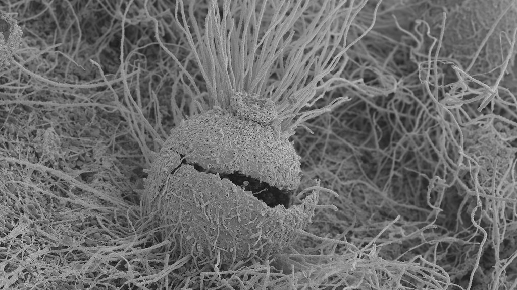
MC² has recently had a major upgrade in electron microscopy instrumentation. The old field emission - scanning electron microscope (FE-SEM) and the tungsten filament scanning electron microscope (SEM) have both been replaced with new instruments and 2 new coating units have also been installed.
New Hitachi SU3900 SEM
The new tungsten filament SEM is an Hitachi SU-3900 large chamber SEM. It is capable of taking samples up to 30 cm in diameter and imaging the central 20 cm of the sample as well as 13 cm height. Samples can be looked at in low vacuum without coating. The SEM also has a 170 mm² Ultim Max EDX and is equipped with secondary and backscatter detectors in both low and high vacuum.
Advantages over the previous SEM are as follows:
- Larger chamber, allowing larger samples to be imaged.
- Higher resolution.
- Very simple software.
- Hitachi 3D software to reconstruct a 3D surface from using 4 of the quadrants of the backscatter detector.
New 170 mm² Ultim Max EDX on SEM and FE-SEM and 100 mm² Ultim Extreme of FE-SEM
The new energy dispersive X-ray analysers attached to both the FE-SEM and SEM have many advantages over the previous EDX:
- 17 times large detector area allowing map data or spectra to be collected in 17 times faster, or with a much lower beam exposure for beam sensitive materials.
- Automation software is included allowing spectra or maps of many different areas or samples to be automatically collected allowing the automated system to be run over night with no operator interaction if needed.
- AZtec Feature particle analysis software is included allowing fast collection and analysis of particles in a sample.
- Automatic image and map montaging to allow large areas of a sample to be imaged or mapped at very high image resolution.
- Ultim Extreme detector fitted to the FE-SEM is optimised for low kV work allowing EDX measurements to be taken from the top few nm on certain samples, with much greater lateral resolution.
Coming in May 2021, Oxford Instruments Symmetry S2 Electron Backscatter diffraction detector on the SEM
An Oxford Instruments Symmetry S2 EBSD detector has been ordered for the SEM and will be delivered in May. EBSD allows Kikuchi electron diffraction patterns to be recorded for every pixel in an SEM image. The Symmetry S2 is a very fast CMOS camera allowing up to 4500 Kikuchi patterns per second to be automatically indexed.
Advantages of EBSD are:
- Crystallographic structure can be determined alongside the elemental analysis given by EDX.
- As well as crystallographic structure, phase, stress, crystal orientation, grain boundaries etc. can also be determined using EBSD.
Upgraded gold coater
The previous chromium coater has been serviced and upgraded with a tilt and rotate stage and repurposed as a higher resolution gold coater. Advantages are:
- The base vacuum of this coater is much higher than the previous gold coater allowing smaller gold particles to be deposited and therefore able to be used at higher resolution.
- The tilt and rotate stage allows samples with more topography to be coated.
New carbon and chromium coaters
New very high resolution carbon and chromium coaters have been purchased: a Quorum Q150T-VE and a Q150T-VS. Advantages over the previous coaters are:
- 3 orders of magnitude better vacuum for the chromium coater allowing samples to be coated and imaged at sub nanometer resolutions required for the new FE-SEM.
- Tilt and rotate stages to allow samples with topography to be coated.
- Ability to coat with carbon fibre for quicker results or with carbon rod for higher resolution coating.
- A glow discharge unit can be fitted into the chromium coater for preparing hydrophobic surfaces on carbon grids for TEM samples.
- Simple method driven operation and so easy for users to prepare their own coatings.
- Both coaters have thickness monitors allowing a controlled amount of coating to be applies. If the thickness of the coating is known this can be compensated for with the EDX software.
New Jeol 7900F FE-SEM
The new FE-SEM is a Jeol JSM-7900F high resolution instrument. Advantages over the old FE-SEM are as follows:
- Much higher resolution. The 7900F has a resolution of 0.7 nm at 1 kV and 0.6 nm at 15 kV.
- Beam deceleration allowing enhanced signals to be achieved at low kV.
- In-lens secondary electron and electron detectors allow secondary and backscattered electrons to be detected at very short working distances (up to 2 mm working distance).
- A 4 quadrant sensitive in-chamber backscatter detector allows backscattered electron to be detected at 800 V and higher accelerating voltages.
- A STEM detector is fitted to allow up to 12 TEM samples to be looked at in the SEM.
- Samples up to 4 inches can be inserted into the FE-Sem via the airlock compared with 32 mm for the old FE-SEM.
- 2 EDX detector are present where the old FE-Sem had none.
- A quorum Cryo system is also fitted.
Quorum PP3010T Cryo prep system for FE-SEM
The FE-SEM has a cryo prep / transfer system attached. Advantages are:
- Beam sensitive sample can be viewed at low temperature causing less damage to the samples.
- Hydrated samples can be imaged without the need to be dried / freeze dried.
- Sample can be flash frozen and transferred via a cryo transfer system directly onto the cryo stage in the FE-SEM and can be coated whilst still frozen.
Access and training
Currently, due to COVID restrictions, we are not offering training on these microscopes, but will aim to restart limited training to superusers on the Hitachi in the next few weeks.
For more information on any of this, please contact Philip Fletcher or Diana Lednitzky.

