Electron microscopy encompasses a number of imaging techniques which use a focused beam of electrons to produce an image, rather than using visible light. Electron microscopy allows for imaging at much higher resolution, with far greater depth of focus than can be achieved using optical methods. Have a look at one of our images that was recently highly commended in the Images of Research competition.
The research facilities have two Scanning Electron Microscopes (SEM) and one Transmission Electron Microscope (TEM). The SEMs produce high resolution images of sample surfaces, whilst the TEM images through the sample.
Scanning Electron Microscopy (SEM)
Hitachi SU3900 Large chamber, variable pressure SEM
This microscope allows easy, intuitive operation, with a specimen chamber that is able to accommodate large samples, and a motorised stage allowing quick and easy specimen positioning. Variable pressure mode enables samples normally unstable in a high vacuum environment, or that have a tendency to charge, to be examined. Pharmaceutical particles, fibres and electronic components may be characterised without coating. A high sensitivity backscattered electron detector is fitted for compositional imaging.
Features include:
- Magnifications up to 30,000x.
- Variable pressure mode - for charging, uncoated and out-gassing samples.
- Large sample chamber: up to 30 cm diameter and 13 cm height.
- Backscattered electron detector for compositional and topographic imaging.
- Fully automated stage controls.
It also has a large area Energy Dispersive X-ray analyser (EDX) attached (Ultim Max 170 mm²), which allows quantitative or semi-quantitative element analysis of materials present in the sample. It also allows X-ray mapping to show the distribution of particular elements across a sample.
JEOL JSM-7900F FESEM
This field emission scanning electron microscope allows for high resolution imaging. Features include:
- Magnifications up to 500,000x.
- Thermal (Schottky) field emission gun (accelerating voltage range 10 V to 30 kV) with a maximum probe current > 500 nA.
- Imaging at low accelerating voltages of 0.01-5 kV.
- Resolution of 0.7 nm at 1 kV and 0.6 nm at 15 kV.
- Samples up to 4 inches can be inserted into the FE-SEM via the airlock.
- In-lens secondary electron and electron detectors allow secondary and backscattered electrons to be detected at very short working distances (up to 2 mm working distance).
- A retractable 4 quadrant sensitive in-chamber backscatter detector allows backscattered electron to be detected at 800 V and higher accelerating voltages.
- A Deben four segment STEM detector to allow up to 12 TEM samples to be looked at in the SEM.
- 2 EDX detectors: Ultim Max 170 mm² and Ultim Extreme 100 mm² at low accelerating voltage for ultimate spatial resolution.
- A Quorum PP3010T Cryo system to view beam sensitive samples at low temperature causing less damage to them.
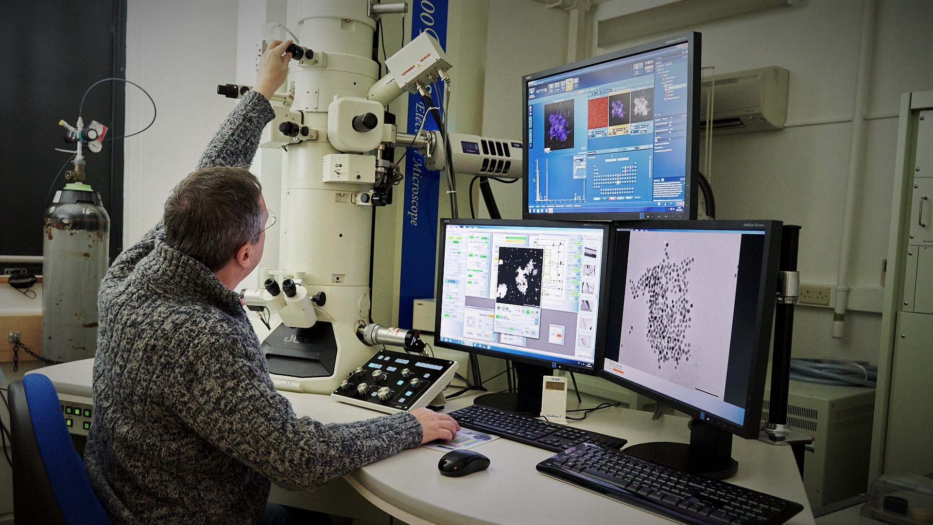
Transmission Electron Microscopy (TEM)
Our JEOL JEM-2100Plus instrument is a multi-purpose transmission electron microscope, combining a JEM-2100 optical system with an advanced control system for enhanced ease of operation. Features include:
- 200 kV maximum operating voltage.
- LaB6 electron gun for excellent performance with reasonable running costs.
- ‘TEM Centre’ control software - an intuitive user interface designed to maximize ease of operation.
- A digital Scanning Transmission Electron Microscopy (STEM) system fully integrated into the TEM, and BF & HAADF detectors.
- Oxford Instruments large area EDX detector and Aztec analysis software for high resolution elemental mapping.
- A high tilt angle sample holder to enable electron tomography.
- A dual tilt beryllium sample holder for analysis and diffraction.
- An integrated JEOL 5 megapixel Ruby digital camera system.
Typical samples are <50 nm thick, nanotubes, nanoparticles, biological samples, material cross sections, and thin samples of bulk material.
Sample Preparation
We also offer a service of ion milling and other sample preparation, including sample coating (gold, chromium and carbon).
